- 您现在的位置:买卖IC网 > Sheet目录3818 > PIC18F4620-I/ML (Microchip Technology)IC MCU FLASH 32KX16 44QFN
1996 Microchip Technology Inc.
DS30412C-page 55
PIC17C4X
9.2
PORTB and DDRB Registers
PORTB is an 8-bit wide bi-directional port. The corre-
sponding data direction register is DDRB. A '1' in DDRB
congures the corresponding port pin as an input. A '0'
in the DDRB register congures the corresponding port
pin as an output. Reading PORTB reads the status of
the pins, whereas writing to it will write to the port latch.
Each of the PORTB pins has a weak internal pull-up. A
single control bit can turn on all the pull-ups. This is
done by clearing the RBPU (PORTA<7>) bit. The weak
pull-up is automatically turned off when the port pin is
congured as an output. The pull-ups are enabled on
any reset.
PORTB also has an interrupt on change feature. Only
pins congured as inputs can cause this interrupt to
occur (i.e. any RB7:RB0 pin congured as an output is
excluded from the interrupt on change comparison).
The input pins (of RB7:RB0) are compared with the
value in the PORTB data latch. The “mismatch” outputs
of RB7:RB0 are OR’ed together to generate the
PORTB Interrupt Flag RBIF (PIR<7>).
This interrupt can wake the device from SLEEP. The
user, in the interrupt service routine, can clear the inter-
rupt by:
a)
Read-Write PORTB (such as; MOVPF PORTB,
PORTB
). This will end mismatch condition.
b)
Then, clear the RBIF bit.
A mismatch condition will continue to set the RBIF bit.
Reading then writing PORTB will end the mismatch
condition, and allow the RBIF bit to be cleared.
This interrupt on mismatch feature, together with soft-
ware congurable pull-ups on this port, allows easy
interface to a key pad and make it possible for wake-up
on key-depression. For an example, refer to AN552 in
the
Embedded Control Handbook.
The interrupt on change feature is recommended for
wake-up on operations where PORTB is only used for
the interrupt on change feature and key depression
operation.
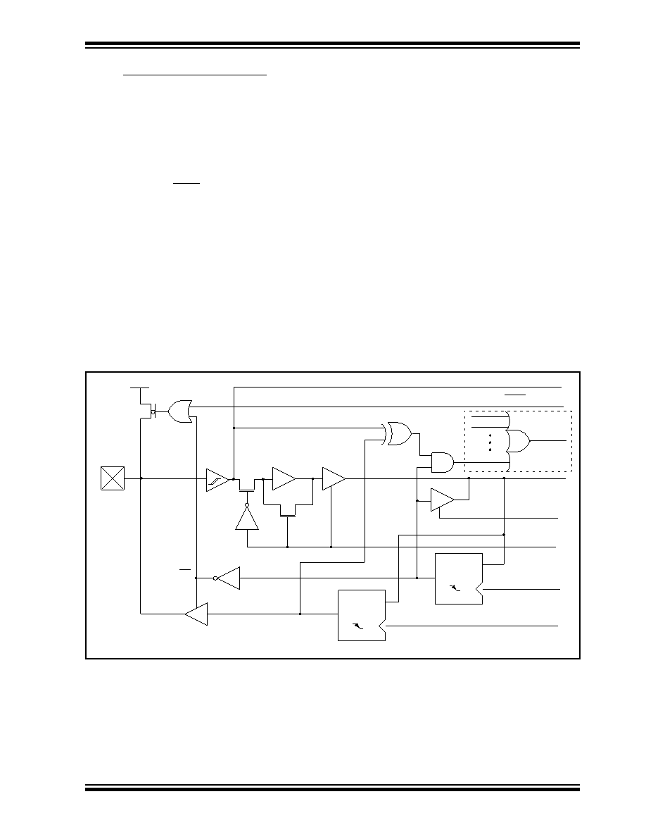
FIGURE 9-4:
BLOCK DIAGRAM OF RB<7:4> AND RB<1:0> PORT PINS
Note: I/O pins have protection diodes to VDD and VSS.
Data Bus
Q
D
CK
Q
D
CK
Weak
Pull-Up
Port
Input Latch
Port
Data
OE
WR_PORTB (Q4)
WR_DDRB (Q4)
RD_PORTB (Q2)
RD_DDRB (Q2)
RBIF
RBPU
Match Signal
from other
port pins
(PORTA<7>)
Peripheral Data in
发布紧急采购,3分钟左右您将得到回复。
相关PDF资料
PIC24HJ256GP210-I/PT
IC PIC MCU FLASH 128KX16 100TQFP
PIC24HJ128GP310A-I/PF
IC PIC MCU FLASH 128KB 100-TQFP
DSPIC33FJ128GP310-I/PF
IC DSPIC MCU/DSP 128K 100TQFP
PIC16C66-20I/SO
IC MCU OTP 8KX14 PWM 28SOIC
DSPIC33FJ128MC510-I/PT
IC DSPIC MCU/DSP 128K 100TQFP
PIC16C66-20I/SP
IC MCU OTP 8KX14 PWM 28DIP
PIC18LF2620-I/SP
IC MCU FLASH 32KX16 28SDIP
PIC16F877-04I/P
IC MCU FLASH 8KX14 EE 40DIP
相关代理商/技术参数
PIC18F4620-I/P
功能描述:8位微控制器 -MCU 64KB 3968 RAM 36 I/O RoHS:否 制造商:Silicon Labs 核心:8051 处理器系列:C8051F39x 数据总线宽度:8 bit 最大时钟频率:50 MHz 程序存储器大小:16 KB 数据 RAM 大小:1 KB 片上 ADC:Yes 工作电源电压:1.8 V to 3.6 V 工作温度范围:- 40 C to + 105 C 封装 / 箱体:QFN-20 安装风格:SMD/SMT
PIC18F4620-I/P
制造商:Microchip Technology Inc 功能描述:IC 8BIT FLASH MCU 18F4620 DIP40
PIC18F4620-I/PT
功能描述:8位微控制器 -MCU 64KB 3968 RAM 36 I/O RoHS:否 制造商:Silicon Labs 核心:8051 处理器系列:C8051F39x 数据总线宽度:8 bit 最大时钟频率:50 MHz 程序存储器大小:16 KB 数据 RAM 大小:1 KB 片上 ADC:Yes 工作电源电压:1.8 V to 3.6 V 工作温度范围:- 40 C to + 105 C 封装 / 箱体:QFN-20 安装风格:SMD/SMT
PIC18F4620-I/PT
制造商:Microchip Technology Inc 功能描述:IC 8BIT FLASH MCU 18F4620 TQFP44
PIC18F4620T-I/ML
功能描述:8位微控制器 -MCU 64KB 3968 RAM 36 I/O RoHS:否 制造商:Silicon Labs 核心:8051 处理器系列:C8051F39x 数据总线宽度:8 bit 最大时钟频率:50 MHz 程序存储器大小:16 KB 数据 RAM 大小:1 KB 片上 ADC:Yes 工作电源电压:1.8 V to 3.6 V 工作温度范围:- 40 C to + 105 C 封装 / 箱体:QFN-20 安装风格:SMD/SMT
PIC18F4620T-I/PT
功能描述:8位微控制器 -MCU 64KB 3968 RAM 36 I/O RoHS:否 制造商:Silicon Labs 核心:8051 处理器系列:C8051F39x 数据总线宽度:8 bit 最大时钟频率:50 MHz 程序存储器大小:16 KB 数据 RAM 大小:1 KB 片上 ADC:Yes 工作电源电压:1.8 V to 3.6 V 工作温度范围:- 40 C to + 105 C 封装 / 箱体:QFN-20 安装风格:SMD/SMT
PIC18F4680-E/ML
功能描述:8位微控制器 -MCU 64KB 3328 RAM w/ECAN RoHS:否 制造商:Silicon Labs 核心:8051 处理器系列:C8051F39x 数据总线宽度:8 bit 最大时钟频率:50 MHz 程序存储器大小:16 KB 数据 RAM 大小:1 KB 片上 ADC:Yes 工作电源电压:1.8 V to 3.6 V 工作温度范围:- 40 C to + 105 C 封装 / 箱体:QFN-20 安装风格:SMD/SMT
PIC18F4680-E/P
功能描述:8位微控制器 -MCU 64KB 3328 RAM w/ECAN RoHS:否 制造商:Silicon Labs 核心:8051 处理器系列:C8051F39x 数据总线宽度:8 bit 最大时钟频率:50 MHz 程序存储器大小:16 KB 数据 RAM 大小:1 KB 片上 ADC:Yes 工作电源电压:1.8 V to 3.6 V 工作温度范围:- 40 C to + 105 C 封装 / 箱体:QFN-20 安装风格:SMD/SMT